|
Product Description:
Patterned Sapphire Substrates (PSS) is micro-patterned sapphire substrate used to for GaN based light emitting diodes(LEDS). The PSS reduces the dislocation density in the GaN layer, enhances the light extraction efficiency and increase LEDs’ brightness.
|
|
|
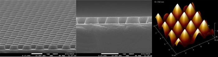
Figure 1: PSS pattern types
|
Features:
- Nano-scale pattern is available
- Dome, pillar or rod types are available
- Custom pattern is welcome
Specification:
| Material |
Mono-crystalline Sapphire Substrate |
| Diameter |
50.8±0.1mm (2 inches) |
100.0±0.2mm (4 inches) |
| Orientation |
C-M axis 0.2°
|
C−>M-axis 0.2° |
| Orientation Tolerance |
± 0.2° |
| Thickness |
430 ± 25um |
650 ± 25um |
| Primary Flat Length |
16.0±1.0mm
|
30.0±1.5mm
|
| Primary Flat Orientation |
A-plane (1 1-2 0 ) ± 0.2° |
| TTV |
≤10µm |
≤15µm |
| BOW |
≤10µm |
≤15µm |
| Front Surface |
Epi-Polished (Ra< 0.2nm) |
| Back Surface |
Fine ground (0.6~1.2μm) or Epi-polished |
| Pattern Height |
0. 45, 1.6, 1.6μm
|
| Pattern Pitch |
1.0, 3.0, 3.0μm
|
| Pattern Bottom Diameter |
0.7, 2.4, 2.6μm
|
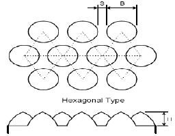
Pattern Arrangement
|
|
| Appearance |
Free of foreigh materials, crack, sawmark, or chipppings |
| Packaging |
Packaged in a class 100 clean room environment |
2 Inch C-M axis 0.2° patterned sapphire wafers in stock, thickness: 0.43mm, one side polished, PPSS-1131171 ($52.0):
|
|
|
|
|
|

|
|
| Pattern height:1.6um, pattern pitch: 3um, pattern bottom diameter:2.5. Primary flat orientation is A-Plane. contact us for quantity pricing. |
2 Inch C-M axis 0.2° patterned sapphire wafers in stock, thickness: 0.43mm, double side polished, PPSS-1131172 ($92.0):
|
|
|
|
|
|
|
|
| Pattern height:1.6um, pattern pitch: 3um, pattern bottom diameter:2.5. Primary flat orientation is A-Plane. contact us for quantity pricing. |
2 Inch C-M axis 0.2° patterned sapphire wafers in stock, thickness: 0.43mm, double side polished, PPSS-1131112 ($108.0):
|
|
|
|
|
|
|
|
| Pattern height: 0.45um, pattern pitch: 1um, pattern bottom diameter: 0.7um. Primary flat orientation is A-Plane. contact us for quantity pricing. |
2 Inch C-M axis 0.2° patterned sapphire wafers in stock, thickness: 0.43mm, one side polished, PPSS-1131151 ($52.0):
|
|
|
|
|
|
|
|
| Pattern height:1.6um, pattern pitch: 3um, pattern bottom diameter:2.6. Primary flat orientation is A-Plane. contact us for quantity pricing. |
4 Inch C-M axis 0.2° patterned sapphire wafers in stock, thickness: 0.65mm, one side polished, PPSS-1361451 ($208.0):
|
|
|
|
|
|
|
|
| Pattern height:1.6um, pattern pitch: 3um, pattern bottom diameter:2.6. Primary flat orientation is A-Plane. contact us for quantity pricing. |
6 Inch C-M axis 0.2° patterned sapphire wafers in stock, thickness: 1.0mm, one side polished, PPSS-14A1581 ($596.0):
|
|
|
|
|
|
|
|
| Pattern height:1.6um, pattern pitch: 3um, pattern bottom diameter:2.6. Primary flat orientation is A-Plane. contact us for quantity pricing. |
|
